
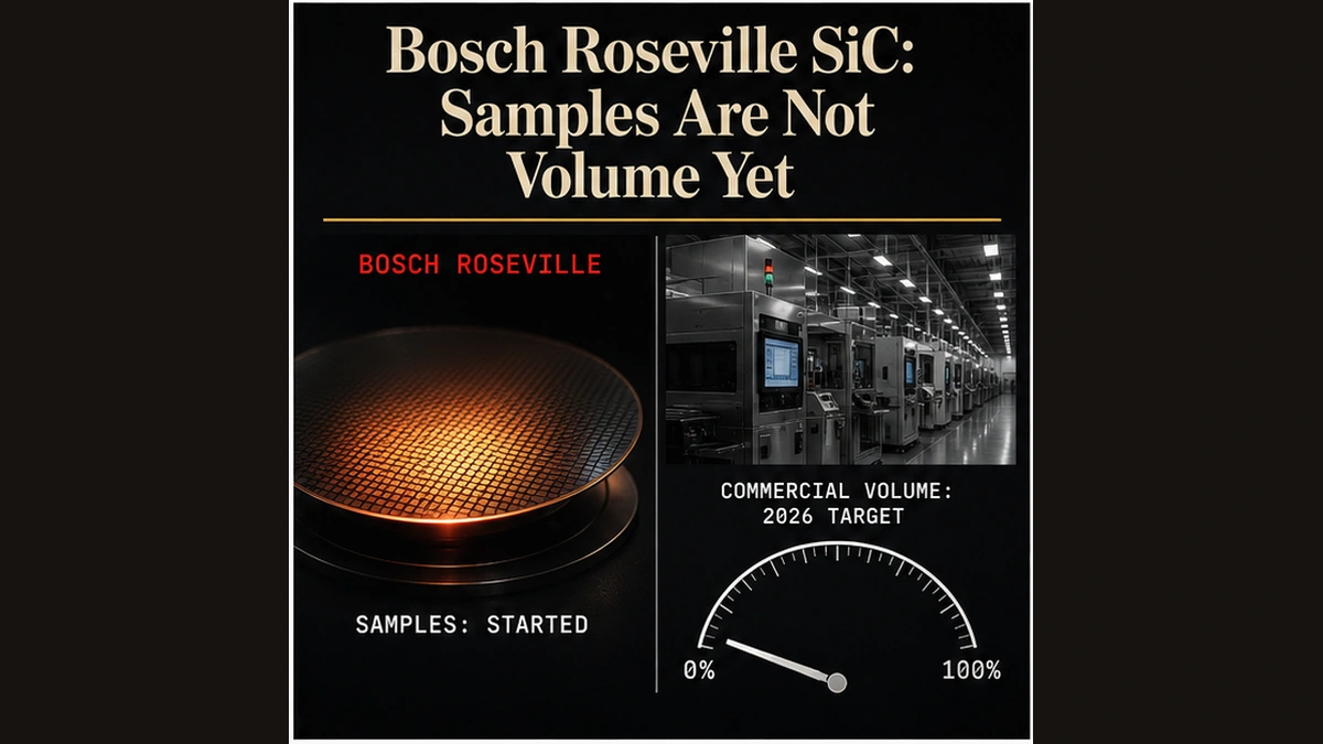
Direct answer – Is Bosch producing silicon carbide chips at commercial volume in Roseville?
Not yet, based on Bosch’s July 2026 announcement. Bosch says sample silicon carbide production has begun at Roseville and commercial production on 200-millimeter wafers is intended to start in 2026. The company did not disclose current yield, qualified monthly output or customer volume in the release.
Bosch said sample silicon carbide production is underway at its Roseville, California facility as it announced a definitive agreement for up to $225 million in direct CHIPS funding.
The company plans to invest up to $2 billion to transform the existing site and intends to begin commercial manufacturing on 200-millimeter wafers in 2026. Roseville is Bosch’s first semiconductor production site in the United States.
The manufacturing question is not whether the project is real. It is what the word production means at this stage. Samples prove that tools and process steps can create wafers; they do not yet prove stable yield, customer qualification or repeatable commercial output.
Key Takeaways
- Bosch has begun sample SiC production at the converted Roseville semiconductor facility.
- Commercial production on 200-millimeter wafers is still planned for later in 2026.
- The Commerce agreement provides up to $225 million toward an investment of up to $2 billion.
- Bosch disclosed no current yield, monthly qualified output or named customer qualification.
- Buyers should track process qualification and good wafer output, not the funding total alone.
What Bosch actually announced in Roseville
The current milestone combines three separate facts. Bosch has a definitive direct-funding agreement, the site has started making sample SiC material and the company still targets commercial manufacturing during 2026.
Bosch acquired the existing Roseville wafer fab in August 2023 rather than building a greenfield shell. The conversion adds a new cleanroom and a new production line for 200-millimeter silicon carbide wafers, with more than 300 associates already working at the site.
That existing industrial base can shorten a project, but it does not remove the qualification sequence. The difference is familiar in Micron’s U.S. memory capacity buildout: construction, equipment installation, process yield and customer-approved supply are distinct milestones.
The $225 million figure also needs context. It is direct CHIPS funding toward an investment Bosch describes as up to $2 billion, not the total cost of the factory and not a statement of current production value.
Why sample production is not commercial output
Sample production is an important engineering gate. It shows the line can run material through the intended process and gives teams physical wafers for metrology, reliability testing, defect analysis, packaging work and customer evaluation.
Commercial output adds tougher requirements. The process must repeat across lots, control defects, hold electrical performance, maintain usable yield and produce enough qualified wafers on schedule. A line can create good samples while still learning how to do that consistently at volume.
Bosch’s release does not provide a current wafers-per-month figure, sample yield, production yield, customer approval date or committed commercial shipment. Those omissions do not show a problem. They show why the safest reading is sample milestone now, commercial ramp later.
A controlled semiconductor quality management system matters during this gap because every process change, deviation, inspection result and corrective action has to remain traceable while the recipe is still moving toward release.
Why the 200-millimeter conversion matters
Silicon carbide devices support high-voltage and high-temperature applications in electric vehicles, charging, data centers, defense and other power systems. Moving SiC production to 200-millimeter wafers can create more device area per wafer than a smaller format, provided the larger process reaches acceptable yield.
Bosch says Roseville will complement its SiC production in Reutlingen and Dresden, Germany. That adds a U.S. manufacturing point to an existing network instead of asking a single new site to carry the entire technology program.
The supply-chain value will still depend on product and process qualification. Domestic geography can shorten some routes and reduce certain risks, but a buyer cannot substitute the words U.S. fab for evidence that the required die, package and reliability profile are approved.
The same rule applies to TTM’s new Ultra-HDI capacity. A facility announcement becomes usable supply only after the relevant process window, inspection evidence, yield and customer approval are demonstrated at the volume a program needs.
What manufacturers and buyers should watch next
The first useful update is Bosch’s commercial-production start, including whether it refers to line release, first customer shipment or sustained output. Those events can occur on different dates, so the wording matters.
The second is qualification evidence. Buyers should look for named device families, customer or application approvals, reliability status and any disclosed transition from engineering lots to production lots. A monthly capacity figure is more useful when it is paired with good yield or qualified output.
The third is conversion progress. A brownfield fab can reuse utilities, infrastructure and a skilled local workforce, but the new cleanroom and SiC line still have commissioning, metrology and process-control gates. Funding finalization helps pay for that work; it does not complete it.
Bosch has crossed a meaningful line by producing samples in Roseville. The next claim manufacturers can act on is narrower and harder: repeatable 200-millimeter SiC output that has passed the qualification required for a specific product and customer.
Frequently Asked Questions
Bosch says it intends to start commercial manufacturing of silicon carbide semiconductors on 200-millimeter wafers in 2026. Its July announcement did not give a more specific date or define whether the milestone means line release, first qualified shipment or sustained commercial volume.
Bosch announced a definitive direct-funding agreement with the U.S. Department of Commerce for up to $225 million. The award supports a planned investment of up to $2 billion to transform the existing Roseville site for silicon carbide semiconductor manufacturing.
Sample production means the process can make physical wafers for measurement, reliability work, packaging development and customer evaluation. It is a real manufacturing milestone, but it does not by itself establish stable yield, qualified monthly output or sustained commercial shipments.
A 200-millimeter wafer offers more usable area than a smaller wafer and can improve manufacturing economics when defect control and yield are strong. The benefit is not automatic: the process must maintain uniformity, reliability and acceptable good-die output across the larger wafer.